
Samsung, ASML team up on next
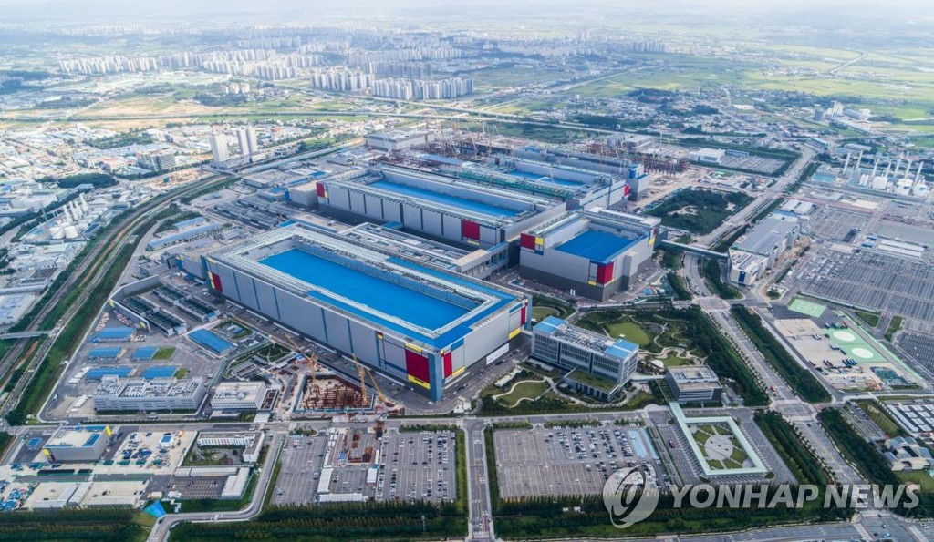
SEOUL, Sept. 8 (Yonha) -- Samsung Electronics Co. said Tuesday that it has joined a consortium led by Netherlands-based semiconductor equipment manufacturer ASML to develop next-generation semiconductor manufacturing technologies.
The partnership aims to advance 12-inch photomask technology for future semiconductor manufacturing, replacing the 6-inch photomask format that has been widely used for decades, the South Korean technology giant said.
"Building on years of successful cooperation, the companies will work together to accelerate the development and deployment of technologies that support the increasing performance and efficiency requirements of advanced semiconductor manufacturing," Samsung said in a press release.
The technology is expected to boost fab productivity and reduce chipmaking costs amid surging demand for artificial intelligence (AI) chips.
"The AI era is transforming the semiconductor industry and increasing the importance of technological innovation across the entire value chain," Samsung Electronics CEO Jun Young-hyun said. "By further strengthening our collaboration with ASML, we are helping lay the foundation for the next generation of AI and semiconductor innovation."
Samsung also plans to introduce ASML's High NA extreme ultraviolet (EUV) lithography technology into high-volume manufacturing of dynamic random-access memory (DRAM) for the first time in the industry by 2028.
High NA EUV is expected to extend the DRAM scaling road map by providing improved resolution, enabling process simplification and greater manufacturing efficiency.
This undated image, provided by Samsung Electronics Co., shows its plant at Pyeongtaek. (PHOTO NOT FOR SALE) (Yonhap)
Related Stories
 Technology
BioInnovation Institute injects €1.3 million each into six startups tackling cancer, disease, pest control and decarbonisation
59 minutes ago
 Technology
Exclusive | AI, chip firms among bidders for flagship Northern Metropolis tech hub at border
59 minutes ago
 Technology
Nordic Technology Group AS (NTG): Company update
59 minutes ago
 Technology
China's Huawei Technologies faces racketeering trial in New York
1 hour ago
 Technology
US designates 15-year
3 hours ago
 Technology
Celltrion Launches Korea
5 hours ago
 Technology
Argentina aims for 2027 launch of RA
6 hours ago
 Technology
Celltrion Teams With Japan's Largest Biocluster to Find Startups
6 hours ago