
Semiconductor Industry in India: Incentives and Key Players
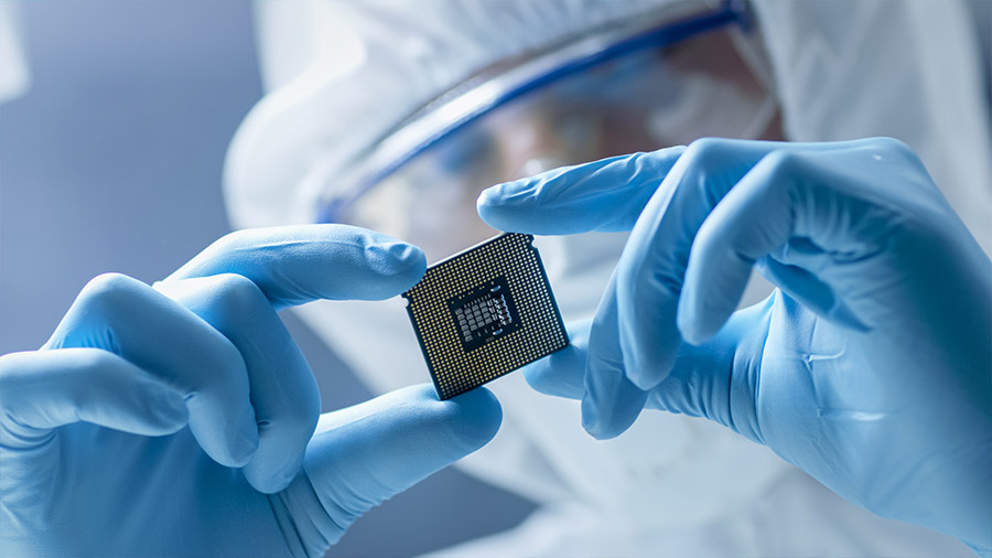
India’s Semiconductor Sector: Tracking Government Support and Investment Trends
India continues to support its semiconductor ecosystem in 2026 with 12 approved projects under the India Semiconductor Mission and one under the Scheme for Promotion of Manufacturing of Electronic Components and Semiconductors. Learn about incentives, key fabs, locations, and investment.
India’s semiconductor manufacturing ecosystem continues to expand in 2026, with 13 approved semiconductor projects operational or under development as of May 18, 2026. The latest addition is an ATMP/OSAT facility in Bhiwadi, Rajasthan, inaugurated on May 15, 2026, under the Scheme for Promotion of Manufacturing of Electronic Components and Semiconductors (SPECS). The facility is notable for being the first semiconductor unit established outside the India Semiconductor Mission (ISM).
India is also strengthening its position within global semiconductor supply chains. On May 16, 2026, Tata Electronics and Dutch semiconductor equipment company ASML signed an agreement to establish India’s first front-end semiconductor fabrication plant in Gujarat.
The growing importance of semiconductors has also extended beyond traditional automotive and consumer electronics applications into sectors such as telecommunications, IoT devices, and medical technology, including MRI systems, wearable health monitors, and diagnostic equipment.
Tata Electronics–ASML partnership for India’s first front-end semiconductor fab
India’s Tata Electronics and Netherland-based ASML signed a strategic agreement on May 16, 2026, to support the development of India’s first front-end semiconductor fabrication facility in Gujarat.
Under the agreement, ASML will provide advanced semiconductor manufacturing technology and equipment for Tata Electronics’ proposed 300-mm wafer fabrication plant being developed in Dholera, Gujarat. The facility, backed by an estimated investment of US$11 billion, is expected to manufacture semiconductor chips for sectors including automotive electronics, mobile devices, industrial applications, and artificial intelligence (AI).
ASML CEO Christophe Fouquet stated that India’s rapidly expanding semiconductor sector presents substantial long-term opportunities, adding that the company intends to deepen its partnerships in the region as the industry matures.
The agreement was formalized during high-level bilateral engagements between India and the Netherlands. As per several media reports, India encouraged greater Dutch investment in strategic industries, including semiconductors, renewable energy, digital infrastructure, and healthcare.
The Tata-ASML partnership aligns with India’s broader semiconductor policy push. Multiple semiconductor projects are currently under development across the country, including large-scale fabrication and packaging facilities led by Tata Electronics in Gujarat.
This collaboration also reflects wider global supply chain realignment trends. Dutch semiconductor companies, including ASML, are increasingly pursuing geographic diversification and new growth markets amid evolving export controls and technology-related trade restrictions linked to ongoing US-China strategic competition.
Rajasthan launches first semiconductor facility
Rajasthan has formally entered India’s semiconductor manufacturing ecosystem with the inauguration of its first semiconductor ATMP/OSAT facility in Bhiwadi on May 15, 2026. Developed under the central government’s SPECS scheme, the project strengthens India’s efforts to expand domestic semiconductor packaging, testing, and electronics manufacturing capabilities.
Sahasra Semiconductors operates the facility, which focuses on semiconductor assembly, testing, marking, and packaging operations. Located within the Bhiwadi electronics manufacturing cluster, the project supports India’s broader semiconductor localization strategy and growing electronics supply chain ecosystem.
CLICK HERE TO KNOW MORE: How Rajasthan’s Bhiwadi Commissioned India’s 13th Semiconductor Unit
India approves two new semiconductor projects under ISM
India’s Union Cabinet has approved two additional semiconductor projects under the ISM on May 5, 2026. The projects include the country’s first commercial mini/micro-LED display manufacturing facility based on Gallium Nitride (GaN) technology, along with a semiconductor packaging and testing unit.
The approved projects will be established in Gujarat with a combined investment of approximately INR 39.36 billion and are expected to create employment opportunities for around 2,230 skilled professionals.
One of the two new approved project, Crystal Matrix Limited, will set up an integrated compound semiconductor fabrication and Assembly, Testing, Marking, and Packaging (ATMP) facility in Dholera, Gujarat. The project will focus on manufacturing mini/micro-LED display modules while also offering GaN foundry services, including epitaxy on six-inch wafers.
The facility is expected to produce 72,000 square meters of mini/micro-LED display panels annually, alongside 24,000 sets of RGB GaN epitaxy wafers. The products are intended for use across multiple applications, including televisions, commercial display systems, smartphones, tablets, automotive displays, XR glasses, and smartwatches.
The second project, Suchi Semicon Private Limited, will establish an Outsourced Semiconductor Assembly and Test (OSAT) facility in Surat, Gujarat, focused on manufacturing discrete semiconductor components. The facility is projected to have an annual production capacity of over 1 billion chips.
The company’s products are expected to support applications in power electronics, analog integrated circuits, and industrial systems, catering to sectors such as automotive, industrial automation, and consumer electronics.
India’s semiconductor push gains momentum with INR 37 billion HCL-Foxconn project
HCL Group and Foxconn have appointed Taiwan-based CTCI Corporation as the engineering, procurement, and construction (EPC) partner for their INR 37.06 billion (US$389.9 million) semiconductor assembly and testing (OSAT) facility in Jewar, Uttar Pradesh.
The facility, being developed under the ISM, will manufacture display driver chips used in smartphones, laptops, PCs, and automotive systems. Located near the upcoming Noida International Airport, the project is expected to generate over 2,000 direct and indirect jobs while strengthening India’s domestic semiconductor packaging and testing capabilities.
CTCI’s appointment also marks its entry into India’s semiconductor sector, building on its existing partnership with Foxconn across projects in Taiwan and the US. Unlike larger fabrication projects underway in Gujarat and Tamil Nadu, the HCL-Foxconn venture will focus on downstream chip packaging and testing — a segment increasingly viewed as critical for improving supply chain resilience and reducing dependence on imported semiconductor components.
Accelerating semiconductor manufacturing through SEZ reforms
On April 9, 2026, the central government notified a Special Economic Zone (SEZ) for Tata Semiconductor in Dholera, Gujarat, enabling the establishment of India’s first semiconductor fabrication facility. The notification formalizes the regulatory framework for the project and designates the zone as an inland container depot, allowing on-site cargo handling and improved logistics efficiency. The move reflects targeted regulatory support to facilitate large-scale semiconductor investments.
India revised the SEZ Rules on June 3, 2025, to ease the establishment of semiconductor and electronics manufacturing units. Key changes included reducing the minimum land requirement from 50 hectares to 10 hectares, relaxing land-related conditions, allowing free-of-cost inputs to count toward export performance, and permitting domestic sales on payment of applicable duties.
Following these reforms, several semiconductor and electronics SEZ projects have been approved across the country. These span fabrication, assembly, testing, and component manufacturing, and are expected to strengthen domestic production, generate skilled employment, and reduce import dependence.
Micron Semiconductor Technology India Pvt. Ltd.
Hubballi Durable Goods Cluster Pvt. Ltd.
Electronics components manufacturing and services
Outsourced Semiconductor Assembly and Testing
Tata Semiconductor Manufacturing Pvt. Ltd.
AI-enabled semiconductor fabrication
Among these, the Tata Semiconductor project in Dholera stands out as India’s first fabrication facility and the largest in terms of investment and scale. Collectively, these developments indicate steady progress toward building a competitive semiconductor ecosystem in India, supported by policy reforms and increasing industry participation.
Sanand strengthens position as a semiconductor hub
Sanand has consolidated its role as a key semiconductor hub with the inauguration of Kaynes Semicon’s OSAT facility on March 31, 2026. Approved under the India Semiconductor Mission, the project involved an investment of INR 33 billion (US$347.9 million) and focuses on chip testing and packaging, with a production capacity of around 6 million chips per day.
This followed the earlier operationalization of Micron’s facility, contributing to rapid industrial growth and expansion of the regional semiconductor ecosystem.
Previously known for automobile manufacturing, Sanand has evolved into a prominent semiconductor cluster, driven by investments from Micron, Kaynes Semicon, and CG Semi. With several projects under the Semicon India Programme located in Gujarat, the region has emerged as a critical node in India’s semiconductor value chain.
India’s semiconductor design and manufacturing ecosystem in 2026
India’s semiconductor market and policy push
India is positioning itself as a trusted alternative hub in global semiconductor supply chains. The domestic semiconductor market was valued at about US$38 billion in 2023 and is projected to reach around US$109 billion by 2030, driven by demand from smartphones, automotive electronics, industrial automation, and data centers.
To reduce import dependence and attract fabrication and advanced packaging investments, the government launched the Programme for Development of Semiconductors and Display Manufacturing Ecosystem in India in 2021, with a total outlay of INR 760 billion (~US$10 billion) and the creation of the India Semiconductor Mission (ISM) as the nodal agency.
Also Read: India’s Semiconductor Sector Outlook 2025: Growth, Investments, and Policy Incentives
Key central schemes and state incentives for semiconductor fabs
Under the umbrella program, multiple schemes support different parts of the value chain:
Several states have rolled out dedicated semiconductor policies on top of central support. For example:
Investors typically structure projects to stack central and state incentives, while meeting localization, technology, and capacity conditions prescribed in the scheme guidelines.
Also Read: India’s Design-Linked Scheme for the Semiconductor Sector: How Businesses Can Maximize Benefits
India semiconductor tracker: Approved semiconductor fab and ATMP/OSAT projects
India now has 13 approved projects; 1 unit under SPECS and 12 under ISM spanning fabs, advanced packaging, and compound semiconductors. The table below consolidates official and widely reported information; values are approximate and rounded.
DRAM & NAND assembly and test; phased ramp-up across two phases.
Approved June 2023 under modified ATMP/OSAT scheme; Phase-1 cleanroom validation underway in 2025; first phase expected to become operational by late 2025 / early 2026.
Tata Electronics (TEPL) + Powerchip Semiconductor Manufacturing Corp (PSMC), Taiwan
Greenfield semiconductor fab (logic/power)
Over INR 915.26 billion (~US$10.1bn)
Up to 50,000 wafers/month, expected nodes around 28 nm and above for power management ICs, display drivers, MCUs, and high-performance logic for automotive, AI, and 5G/compute.
Approved Feb 2024 under semiconductor fab scheme; construction has started.
Commercial operations targeted for FY 2029–30.
State is also enabling worker and supplier housing around the project.
Tata Semiconductor Assembly and Test Pvt Ltd (TSAT)
Up to 48 million chips per day for automotive, EV, and mobile/consumer segments.
Approved Feb 2024 under ATMP/OSAT scheme; land leased for 60 years; first chips targeted around 2025–26 along with co-located skill development center.
CG Power & Industrial Solutions + Renesas (Japan) + Stars Microelectronics (Thailand)
Over INR 76 billion (~US$900mn)
Designed for up to 15 million chips per day at full ramp; first OSAT pilot line (G1) can handle ~0.5m units/day, with G2 lifting capacity to ~14.5m units/day.
Approved Feb 2024; first OSAT pilot line at Sanand inaugurated August 2025 and expected to go into commercial production in 2026.
Kaynes Semicon Pvt Ltd (Kaynes Technology subsidiary)
Capacity of around 6 million chips per day, ramped in phases for industrial, telecom, EV, and consumer applications.
Approved Sept 2024; by Oct 2025 Kaynes has delivered its first India-made chip modules to customers, marking one of the earliest commercial outputs under ISM.
In late September, UST, an AI and technology transformation solutions firm, announced its investment in Kaynes Semicon.
HCL Group – Foxconn JV (Vama Sundari Investments)
Near Jewar Airport, YEIDA Sector 28, Uttar Pradesh
Planned capacity of 20,000 wafers/month, producing around 36 million display driver chips per month for mobiles, laptops, automotive electronics, and other devices.
Approved by Union Cabinet in 2025 as the sixth ISM facility; commercial production expected by 2027. YEIDA has re-allotted a 48-acre plot with supporting infrastructure.
Silicon Carbide (SiC) fab + ATMP
Info Valley, Bhubaneswar, Odisha
First commercial SiC fab in India; about 60,000 SiC wafers/year plus ATMP capacity of ~96 million units/year for high voltage applications in electric vehicles, renewable energy, smart grid systems, data centers, and other industries.
Approved Aug 2025 as one of four new projects; strengthens India’s advanced materials semiconductor base. Expected to be operational by 2027-28.
Expected output: approximately 69,600 glass panel substrates, 50 million assembled units, and 13,200 3DHI modules per year. Proposed products will have applications in defense, high-performance computing, artificial intelligence, RF and automotive, photonics and co-packaged optics etc.
Approved Aug 2025 under compound semiconductors/ATMP scheme, adding critical packaging materials capability within India.
Continental Device India Ltd (CDIL)
Discrete / legacy chips & packaging
Additional capacity of about 158.38 million units/year, largely for discrete semiconductors and legacy devices (MOSFETs, IGBTs, Schottky Bypass Diodes, and transistors, both in Silicon and Silicon Carbide).
Expansion of existing facility under ISM; leverages long-standing local ecosystem in Mohali.
Advanced System in Package (ASIP) Technologies
Advanced SiP & system-in-package
~INR 4.68 billion (≈INR 468 crore)
Planned capacity of around 96 million units/year, focusing on advanced SiP modules for communications and high-density electronics (mobile phones, set-top boxes, automobile applications, etc.).
Approved Aug 2025; strengthens India’s high-end packaging and system-integration capabilities.
Semiconductor fabrication and ATMP
GaN foundry services, including epitaxy on 6” wafers. Additionally, the facility is expected to produce 72,000 square meters of Mini/Micro-LED display panels annually, alongside 24,000 sets of RGB GaN epitaxy wafers
Suchi Semicon Private Limited (SSPL)
Proposed production capacity is 1033.20 million chips per annum. Target applications include power electronics, analog ICs, and industrial systems, serving end markets such as automotive, industrial automation, and consumer electronics.
Received union cabinet approval on May 5, 2026
The facility will package memory chips for products such as micro SD and flash storage, along with LED driver ICs, eSIMs and RFID products.
The unit currently has an annual packaging capacity of 60 million semiconductor units, with plans to scale up to nearly 400-600 million units annually over the next 2-3 years.
Formally inaugurated on May 15, 2026
Beyond ISM-approved units, several moves are reshaping India’s broader semiconductor ecosystem:
For foreign investors, these developments mean that domestic talent, tools, and upstream/downstream suppliers are growing alongside fabrication and OSAT capacity, reducing first-mover risk.
Practical considerations for foreign investors planning a fab or OSAT unit in India
For companies looking to enter or expand in India’s semiconductor and display manufacturing ecosystem, the India Semiconductor Mission scheme offers a compelling opportunity – but success will depend on early clarity and rigorous preparation. To capitalize on this support, foundational steps should include: (1) conducting a detailed feasibility study that aligns the project with the subsidy slabs (e.g., 28 nm or below vs other nodes) and internal rate of return; (2) verifying eligibility criteria – especially investment size and revenue history – and ensuring the corporate vehicle and strategy are structured accordingly; (3) preparing a credible deployment and technology-upgrade roadmap (showing how you’ll evolve in node/device complexity) and tie-up with global supply-chain partners; and (4) ensuring that project scheduling, state-level clearances (e.g., land, utilities) and local ecosystem support (skilling, logistics) are ready. One key advisory point: while the headline rate is up to half the cost, the actual quantum and timing of support is conditioned on milestones, node-size eligibility and government appraisal. Thus, for an investor or technology firm eyeing this scheme: don’t treat the subsidy as simply a grant – embed it into your financial model, stress-test the project without it, and assume you must meet high conditionality. By doing so you can position your business to not only qualify for the incentive but build a resilient manufacturing footprint in India’s growing electronics ecosystem. — Dezan Shira & Associates India
When planning a semiconductor project in India, foreign investors typically need to structure decisions around four pillars:
Q1. What is the India Semiconductor Mission (ISM)?
A. ISM is a specialized agency under the Digital India Corporation tasked with implementing India’s INR 760 billion semiconductor and display manufacturing program. It appraises proposals for fabs, compound semiconductors, ATMP/OSAT units, and design projects, and administers fiscal support of up to 50 percent of project cost under various schemes.
Q2. How many semiconductor projects has the Indian government approved so far?
A. As of May 18, 2026, the central government has approved 13 semiconductor projects across seven states under ISM and SPECS. These include one large logic/power fab, multiple OSAT/ATMP units, and new silicon carbide and substrate-focused projects.
Q3. What level of incentives can semiconductor investors get in India?
A. For eligible projects, the central government provides up to 50 percent of project cost or capital expenditure for fabs, compound semiconductor units, and ATMP/OSAT facilities, plus up to 50 percent reimbursement of design costs (capped) under the DLI scheme. States then layer their own incentives via capital subsidies, land support, power-tariff benefits, and training subsidies.
Q4. Which locations are emerging as India’s main semiconductor hubs?
A. Gujarat (Dholera and Sanand) is becoming the flagship hub with the Tata–PSMC fab and multiple OSAT and ATMP units from Micron, CG Power, and Kaynes. Assam (Jagiroad), Uttar Pradesh (Jewar), Odisha (Bhubaneswar), Punjab (Mohali), and Andhra Pradesh are also hosting approved projects under ISM, supported by tailored state policies and infrastructure plans.
Q5. Are there opportunities for fabless and design-only semiconductor firms in India?
A. Yes. The Design Linked Incentive (DLI) Scheme supports fabless startups and design houses through reimbursement of up to 50 percent of design costs and access to EDA tools and shared infrastructure, while India’s large base of chip design engineers and R&D centers (AMD, NXP, etc.) creates a strong ecosystem for collaboration.
Archive: Semiconductor schemes in India
Link to PDF: Gazette Notification on Thursday, December 30, 2021.
Link to Press Release dated January 16, 2022: Applications invited under the Design Linked Incentive (DLI) Scheme from domestic semiconductor chip design firms
A dedicated portal has been made available – www.chips-dli.gov.in – for inviting online applications from January 1, 2022 to December 31, 2024. The applicants can find the guidelines of the DLI Scheme on the portal and register themselves for availing support under the scheme.
On September 21, 2022, the Cabinet, chaired by Prime Minister Narendra Modi, approved key modifications to the Program for Development of Semiconductors and Display Manufacturing Ecosystem in India:
Under the modified program, a uniform fiscal support of 50 percent of project cost shall be provided across all technology nodes for setting up of semiconductor fabs. Given the niche technology and nature of compound semiconductors and advanced packaging, the modified program shall also provide fiscal support of 50 percent of capital expenditure in pari-passu mode for setting up of compound semiconductors/silicon photonics/sensors / discrete semiconductors fabs and ATMP/OSAT.
This article was originally published on April 6, 2021. It was last updated May 18, 2026.
Entering or expanding in India requires careful assessment of market conditions, regulatory frameworks, and sector competitiveness. Business intelligence insights help companies evaluate opportunities, benchmark competitors, and align investment strategies with India’s evolving economic landscape.
India Briefing is one of five regional publications under the Asia Briefing brand. It is supported by Dezan Shira & Associates, a pan-Asia, multi-disciplinary professional services firm that assists foreign investors throughout Asia, including through offices in Delhi, Mumbai, and Bengaluru in India. Dezan Shira & Associates also maintains offices or has alliance partners assisting foreign investors in China, Hong Kong SAR, Vietnam, Indonesia, Singapore, Malaysia, Mongolia, Dubai (UAE), Japan, South Korea, Nepal, The Philippines, Sri Lanka, Thailand, Italy, Germany, Bangladesh, Australia, United States, and United Kingdom and Ireland.
For a complimentary subscription to India Briefing’s content products, please click here. For support with establishing a business in India or for assistance in analyzing and entering markets, please contact the firm at india@dezshira.com or visit our website at www.dezshira.com.
Related Stories
 India
India
News Live: Watch Times Now Live Streaming | Live News India, World, Politics, Sports News
4 hours ago
 India
India
"More than a rockstar": Indian diaspora in Oslo eagerly awaits PM Modi's arrival
4 hours ago
 India
India
Global Indian Diaspora Alliance (GLO
4 hours ago
 India
India
What is Operation Tiger? The MP ‘rebellion’ rocking Shiv Sena
3 days ago
 India
India
India: Why a country of 1.4 billion is not in the football World Cup
3 days ago
 India
India
News Live: Watch Times Now Live Streaming | Live News India, World, Politics, Sports News
3 days ago
 India
India
Indian outrage over US killing of sailors mounts as leaders attend G7 summit
3 days ago
 India
India
Grateful for your concern about Indian diaspora: PM Modi to Canadian PM | He invited PM Modi to visit Canada | Inshorts
3 days ago